

From SMD to COB: A Complete Map of Display Packaging Technology Evolution
One,LED Packaging Technologysummarize
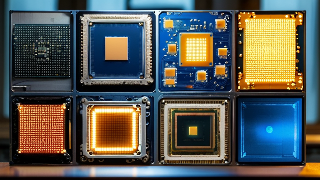
As the core link of modern display technology, LED encapsulation directly affects the brightness, color reproduction and service life of the display. Encapsulation process through the LED chip fixed on the substrate, the establishment of electrical connections and the imposition of a protective layer, so that the tiny chip into a stable working display unit. The current mainstream SMD, COB, IMD three major packaging systems, corresponding to different application scenarios and technical characteristics.
Second, the mainstream packaging technology comparison
1. SMD Surface Mount Technology
The RGB three-color chips are encapsulated into individual lamp beads using precision SMD process and fixed on the PCB substrate through surface mounting technology. Its advantages are:
- Supports P1.0-P4.0 dot pitch range
- Single-lamp interchangeable for low maintenance
- Mature industry chain support
However, there are problems such as easy oxidation of solder joints and limited contrast.
2. COB integrated package
Multiple chips are directly bound to the substrate after the overall package, eliminating the need for traditional bracket structure. Core advantages are reflected in:
- Contrast ratio increased to 10,000:1
- Protection class up to IP54 standard
- Supports 0.4mm ultra-micro pitch
The main challenges are rework difficulties and mass production yield control.
3. IMD composite technology
Innovative fusion of SMD and COB technology features with matrix integrated packaging solution. Via:
- 4-in-1/6-in-1 Chip Integration
- Nano-scale surface coating
- Secondary Optical Design
Successfully realized high reliable display at P0.6 ultra-micro pitch.
III. Key process flow analysis
1. Solidification process: Adoption of high-precision solid crystal machine, through the silver glue or eutectic process to locate the chip within the 0.01mm precision range Epoxy or silicone encapsulation requires a balance of transmittance (>92%) and thermal expansion. 1. Miniaturization Breakthrough: Flip Chip Technology Realizes Sub-50μm Chip Packaging With the breakthrough of Mini/Micro LED technology, the package form continues to evolve:
2. Wire bonding process: Gold or alloy wire bonding, wire arc height control at 120-150μm
3. dispensing package
4. spectral screening: Optical parameter grading by wavelength ±1.5nm, brightness ±5%IV. Technology development trends
2. material innovation: Aluminum Nitride Substrates, Quantum Dot Phosphor Applications
3. Intelligent production: AI Vision Inspection System keeps defective rate below 50PPM
4. Thermal optimizationMicrochannel liquid cooling technology increases power density to 3W/cm².V. Application Scenario Evolution